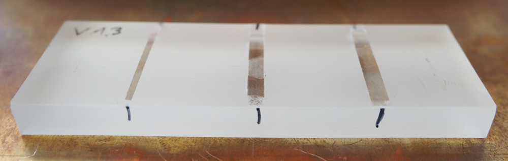
Etching means the step by step removal of surface layers with chemical or physical processes. Depending on the etching process a distinction is made between wet-chemical or dry-physical etching, but there are also combinations of both. In classical wet-chemical etching the substrate surface to be etched is brought into contact with a corrosive solution. In the here used dry-chemical etching, radicals generated in a plasma chamber react with the substrate surface atoms forming gaseous molecules and avoiding damage to the microstructures. By choosing the feed gases for the plasma the process can be made very selective, as for example, Silicon in an integrated chip does not form volatile products with oxygen.
Photoresists are used in industry for lithographic processes to produce surface structures in the sub-micrometer range. One important field of application is the microsystem technology, which deals mainly with the development and production of semiconductor devices or micromechanical components. In the photolithography a light sensitive polymer (resist) is cured by targeted UV light. The resist acts as shaping die during coating processes or as a protection for the underlying surface during etching processes. After the manufacturing process the cured polymer has to be removed. Etching of the resist pattern poses an extreme challenge, as the microstructures must not be damaged. Today, the removal of cured photoresists takes place via dry-chemical etching processes.

Steffen Pauly M.Sc.
Ph. D. Student, Plasma Technology

Andreas Schulz
Dr.-Ing.Research associate, Plasma Technology